
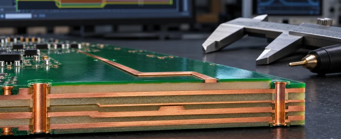
AI-generated editorial illustration of a multilayer PCB stackup and controlled-impedance planning.
A controlled-impedance note added after routing often creates avoidable rework. A trace width selected from a generic online calculator may no longer produce the intended impedance when the fabricator’s actual prepreg thickness, copper build and dielectric data are applied. Changing the width after layout can then disturb clearances, differential spacing, via transitions and timing.
The safer sequence is collaborative: define the electrical targets, obtain a manufacturable stackup, calculate geometry against that construction, route the board, and freeze the agreed data before release. The seven decisions below should therefore be resolved before or at the start of layout—not after the Gerbers are complete.
Why impedance cannot be separated from the stackup
A PCB transmission line consists of a conductor, one or more reference planes and the dielectric between them. Its characteristic impedance depends on the structure and on physical and electrical properties including trace width and finished thickness, distance to the reference plane, dielectric constant, differential spacing and, for surface structures, solder mask and surrounding copper. Polar Instruments summarizes the same relationship in its controlled-impedance application notes.
That is why “route this net at 50 ohms” is incomplete. The number may be the right target, but it does not tell the fabricator which layer, reference plane, geometry, tolerance or material model the designer intended. Typical interface targets such as 50 Ω single-ended or 90/100 Ω differential are examples, not universal defaults; the interface specification and signal-integrity analysis govern the actual requirement.
The pre-layout agreement: seven items
| Item to agree | Questions to answer | Risk if left open |
|---|---|---|
| 1. Impedance target and tolerance | Single-ended or differential? Nominal value? Tolerance and measurement expectation? | Different assumptions at design, CAM and acceptance |
| 2. Signal layer and structure | Microstrip, embedded microstrip, stripline or coplanar? Which layers carry each class? | Wrong field-solver model or geometry |
| 3. Reference plane | Which adjacent plane provides the return path? Is it continuous through the route? | Impedance discontinuities and return-path problems |
| 4. Material system and dielectric data | Which qualified laminate family? Which Dk basis and frequency are used for calculation? | A generic material value produces a non-transferable width |
| 5. Copper and dielectric construction | Finished copper thickness? Pressed dielectric height? Overall thickness and layer count? | The fabricated geometry differs from the calculator input |
| 6. Adjustment authority | May CAM tune trace width or spacing? What changes require designer approval? | Uncontrolled geometry changes or repeated engineering questions |
| 7. Verification and acceptance | Coupon or on-board trace? TDR report? Sampling, records and disposition for out-of-tolerance results? | “Controlled impedance” without an agreed acceptance method |
1. Specify the electrical requirement, not only a label
Create an impedance table that maps every signal class to its target, tolerance, layers and reference plane. Distinguish single-ended impedance from differential impedance and include the intended pair spacing where it is a controlled variable. If the interface standard sets the value, cite the interface and its applicable revision; if simulation produced the requirement, keep the model assumptions with the design record.
A tighter tolerance is not automatically better. It can reduce process latitude, constrain material choices and increase engineering or test effort. Choose a tolerance that the electrical design needs and the intended fabrication process can hold, then make the acceptance rule explicit.
2. Lock the return path and layer assignment
The reference plane is part of the transmission line. A nominally correct trace can still perform poorly if it crosses a plane split, changes reference without a suitable return path or is moved to another layer during layout. Agree the signal-to-plane relationship in the stackup and protect it in the routing rules.
For differential pairs, do not treat the two traces as isolated 50 Ω lines unless that is the intentional model. Pair spacing, trace-to-plane height and coupling all affect differential and common-mode behavior. The field-solver structure must match the actual routed geometry.
3. Use production material data and finished geometry
“FR-4” describes a broad material class, not one universal dielectric constant. Dk varies by resin system, glass style, resin content, test method and frequency. The value used for impedance modeling should therefore come from the proposed material system and the fabricator’s modeling practice, not a single generic number copied between projects.
Copper also needs a consistent definition. Base foil weight alone may not equal the finished conductor thickness after plating, while etching changes the conductor cross-section. Likewise, nominal prepreg thickness is not necessarily the pressed dielectric height in the finished stack. Ask the fabricator to return the proposed construction and calculated production geometry.
4. Decide what the fabricator may tune
There are two common collaboration models. In one, the designer fixes the stackup and the manufacturer tunes the controlled trace width or differential spacing within agreed limits. In the other, routing geometry is fixed and the manufacturer proposes dielectric thicknesses that meet the target. Either can work, but the adjustable variables and approval thresholds must be documented.
Before routing, send the layer count, board thickness, copper requirements, material constraints and impedance table. Route only after receiving a feasible stackup and geometry recommendation. At release, compare the fabrication notes, Gerber/ODB++ data and stackup drawing so they carry one consistent set of values.
5. Plan coupon testing and records
Direct measurement of product traces is often impractical because routes are short, branched or inaccessible and test pads would disturb the structure. A controlled-impedance coupon is fabricated on the same panel with representative layer, line width, copper and dielectric construction. Time-domain reflectometry (TDR) can then evaluate that test structure.
Polar notes that coupon accuracy depends on reproducing the board construction and panel conditions. A coupon is evidence of process and construction consistency; it is not a substitute for correct routing, continuous reference planes or sound via transitions on the product. Agree coupon type, impedance classes, test frequency or method where relevant, sampling and the report supplied with the order.
A practical release checklist
- Impedance table with signal class, target, tolerance, structure, signal layer and reference plane.
- Approved stackup showing material family, finished copper and finished dielectric heights.
- Controlled widths and differential spacings reflected in the layout rules and production data.
- Clear statement of which dimensions CAM may adjust and which require written approval.
- Notes for solder mask, coplanar ground and unusual constructions that affect the model.
- Coupon/TDR requirement, sampling plan, record format and nonconformance disposition.
- Revision-controlled stackup drawing supplied with the Gerber/ODB++ package.
Cost and lead-time implications
Controlled impedance does not add one fixed surcharge. Cost can change through material choice, layer count, dielectric availability, line-width limits, engineering review, coupons and testing. A stable, fabricator-reviewed stackup lets the quotation reflect the real construction. A late impedance requirement may trigger material changes, CAM questions or a complete reroute, making the schedule less predictable.
Frequently asked questions
Can I calculate the trace width before choosing a fabricator?
You can estimate it for floorplanning, but final routing rules should use a manufacturable stackup and production material assumptions confirmed with the selected fabricator.
Should the Gerber note contain only “50 Ω controlled impedance”?
No. Identify the nets or aperture/feature class, layers, reference planes, target, tolerance and verification requirement. Include a stackup drawing.
May a fabricator change controlled trace widths?
Only under an agreed rule. Many fabricators tune geometry to their characterized process, but the allowed range and approval point should be defined before release.
Does a passing coupon prove every high-speed route is correct?
No. It supports fabrication-process verification. Product routing, plane continuity, transitions and connector launches remain design responsibilities.
Review the stackup before routing is frozen
Share layer count, thickness, copper, material constraints and the impedance table when requesting a PCB quotation. JEXPCB can review the proposed construction and confirm project-specific manufacturing and test details before release.
Explore PCB fabrication services · See the PCB quotation file checklist · Request a quote
Technical references
- Polar Instruments AP121: Transmission-line configurations
- Polar Instruments AP124: Testing controlled-impedance boards with coupons
- Polar Instruments: PCB stackup application notes
Technical references checked 27 October 2026.