
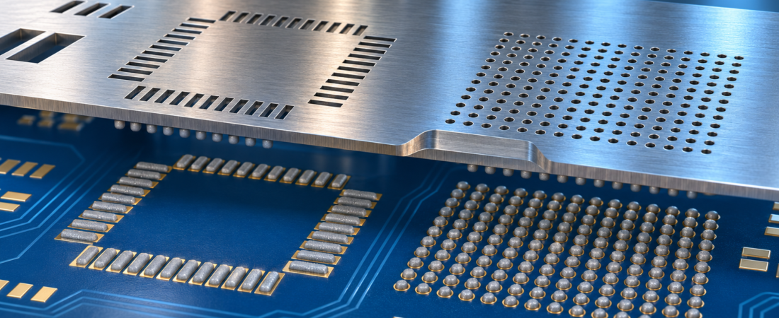
PCB Assembly / Solder paste printing
A stencil is not simply a sheet of metal with every PCB pad copied at 1:1 scale. Its thickness, aperture geometry and local treatment determine how much solder paste reaches each joint and how consistently that paste releases. Fine-pitch leads, QFN thermal pads and micro-BGA arrays often require different deposit volumes on the same board, so the stencil must balance several competing needs.
Approve the stencil from the assembly data, not from the paste layer alone. Review the actual component package, pad geometry, stencil thickness, aperture area ratio, paste type and the smallest and largest deposits on the board before fabrication.
1. Stencil design starts before the laser cuts
The paste Gerber tells the stencil supplier where openings were drawn, but it does not prove that those openings will print reliably. IPC-7525 provides guidance for stencil design and fabrication while emphasizing that printing performance depends on multiple variables rather than one universal rule. [1]
A useful design review should include the fabrication data, assembly drawing, centroid or pick-and-place file, BOM and package drawings for critical components. It should also identify the solder paste alloy and powder class, the intended printing equipment, the reflow atmosphere where relevant, and whether solder-paste inspection (SPI) is available.
| Input | Why it matters | Typical design decision |
|---|---|---|
| Smallest aperture and pitch | Controls paste release and bridge risk. | Foil thickness, aperture reduction, corner radius and paste powder size. |
| Largest component demand | Large terminals and coplanarity variation may need more paste. | Local overprint, step-up area or preform review. |
| QFN exposed pad | Excess paste can float the package and trap volatiles. | Window-pane pattern, coverage target and thermal-via treatment. |
| BGA pad array | Deposit uniformity matters across hundreds of joints. | Round or square apertures, area ratio and positional accuracy. |
| Board support and tooling | PCB movement changes gasket contact and print repeatability. | Fiducials, stencil frame, support pins and keep-out review. |
2. Area ratio links aperture size to stencil thickness
Paste must separate from the aperture walls and remain on the PCB pad when the stencil lifts. The area ratio compares the aperture opening area with the area of its sidewalls. For a rectangular aperture with sides a and b and foil thickness t, it can be expressed as ab / [2(a+b)t]. For a circular aperture of diameter D, the simplified expression is D / 4t.
An industry rule of thumb is to keep the area ratio around 0.66 or higher for a stable release window. IPC technical work also shows that newer pastes, premium foils and coatings may print below this value, but a lower ratio narrows the process window and should be validated rather than assumed. [2] [3]
This is why simply reducing every fine-pitch aperture can backfire. A smaller opening deposits less paste, but it also reduces area ratio. Sometimes a thinner stencil is the better correction. The final choice must still leave enough volume for larger joints elsewhere on the assembly.
3. Package-specific aperture strategies
Fine-pitch gull-wing leads
For fine-pitch QFP and similar leads, the objective is a narrow, repeatable deposit without paste connecting adjacent pads. A small reduction from the copper-pad width, rounded aperture corners and controlled aperture length are common starting points. Home-plate or modified apertures may be used where solder beading or component geometry justifies them, but they should not be added mechanically to every footprint.
Check the solder-mask registration and the real separation between adjacent apertures. If the web between openings becomes too narrow for the selected foil and laser process, stencil strength and dimensional stability may become the limiting factors.
QFN and LGA exposed pads
A large 1:1 opening under a QFN thermal pad can print one thick mass of paste. During reflow this may promote package float, excessive voiding, solder escape toward the perimeter or uneven stand-off. A segmented window-pane pattern divides the deposit into smaller volumes and creates paths for gases to escape.
Coverage is application-dependent. A common engineering starting range is roughly 50–80% of the exposed-pad area, but the correct target depends on the package datasheet, thermal requirement, via pattern, paste and reflow process. Thermal vias inside the pad must be reviewed together with the stencil: open vias can drain paste, while filled and capped vias behave more like a solid pad.
BGA and micro-BGA arrays
BGA joints depend on deposit consistency across the entire array. Round or rounded-square apertures are normally preferred, with dimensions chosen from land geometry, ball size and the area-ratio limit. A 1:1 aperture may be suitable for some packages; others need a slight reduction or a thinner foil to prevent bridging while maintaining release.
Do not compensate for an unfavorable area ratio by specifying a finer paste powder alone. Finer powder can improve filling of small openings, but its higher surface area changes oxidation sensitivity and flux demand. Indium notes the trade-off between fine powder, oxide load and graping risk. [4]
4. One board may need more than one paste height
Many assemblies combine 0.4 mm-pitch devices with shield tabs, connectors, power packages or components whose leads are less coplanar. A thin foil supports small apertures but may underprint the larger joints. A thick foil helps large terminals but can push fine-pitch area ratios below a stable range.
Possible solutions include:
- a step-down stencil around fine-pitch components;
- a step-up region for selected high-volume joints;
- local aperture overprint where spacing permits;
- premium or electroformed foil and a release coating;
- separate printing or solder preforms for exceptional deposits.
Step regions need clearance from nearby apertures and from the squeegee path. The transition must be manufacturable, and the expected paste height should be stated rather than left to interpretation. IPC research describes automated design checks that flag low area ratios and highlights the role of foil technology, coatings and local thickness choices. [2]
5. Release a stencil specification that can be verified
| Specify or approve | What to record |
|---|---|
| Foil | Material, nominal thickness, step regions and any coating. |
| Apertures | Critical reductions or enlargements, window patterns, corner radii and minimum area ratio. |
| Identification | PCB revision, paste-layer revision, stencil side, panel orientation and serial or version control. |
| Tooling | Frame type, fiducials, panel rails, underside support and keep-outs. |
| Process validation | Target transfer efficiency or SPI limits for critical deposits, plus first-article review criteria. |
The stencil drawing should clearly mark every non-1:1 modification. Before volume production, review actual SPI data rather than relying only on nominal aperture dimensions. Stable average volume is not enough if deposit-to-deposit variation, positional offset or edge bridging remains high. For fine-pitch LGA, QFN and micro-BGA printing, AIM also recommends a controlled, low separation speed as part of the printing setup. [5]
Provide Gerber or ODB++ data, assembly drawing, BOM, centroid file, panel drawing, critical package datasheets and any existing stencil or SPI report. Highlight the smallest pitch, QFN exposed pads, BGA arrays and components that previously showed opens, bridges or voiding.
- IPC-7525B — Stencil Design Guidelines.
- IPC technical paper — Selecting Stencil Technologies to Optimize Print Performance.
- IPC technical paper — Quantifying Stencil Aperture Wall Quality.
- Indium Corporation — Minimizing Graping.
- AIM Solder — Solder Paste Print Setting Recommendations.
Need a stencil and assembly DFM review?
JEXPCB can review paste-layer geometry, component packages, panelization and critical solder-joint risks before PCBA production.
Send your assembly data