
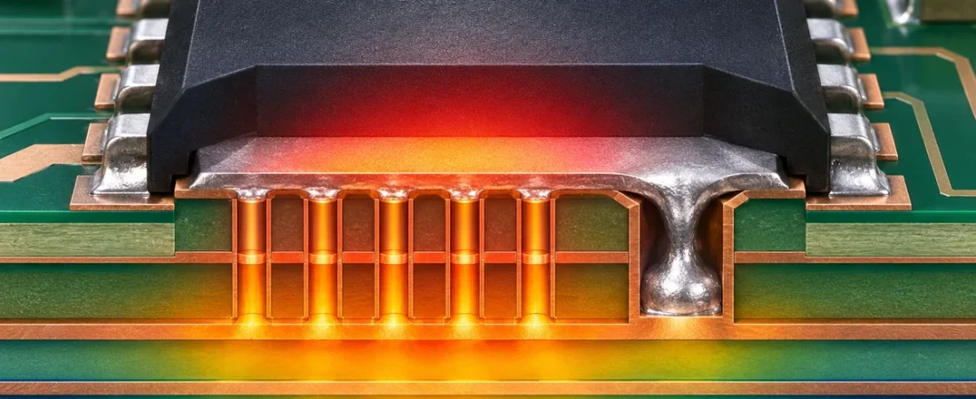
For exposed-pad ICs and many power packages, the PCB is part of the thermal path. Heat must move from the package pad into surface copper, via barrels and internal or bottom-side planes. A thermal via array can lower board thermal resistance, but open holes inside a solderable pad can also remove solder, change stand-off and create voids or solder beads.
There is no universal via count. Package size, power loss, copper thickness, layer stack, airflow, interface material and assembly process all matter. Start with the component manufacturer’s land-pattern and thermal guidance, then validate the complete product.
1. Begin with the package thermal path
Confirm whether the exposed pad is electrically ground, power or another potential, and connect every thermal structure accordingly. Match the top thermal land to the package guidance and provide continuous copper paths into appropriate planes. Thermal-relief spokes increase thermal resistance and are usually inappropriate for dedicated heat-transfer vias unless the vendor says otherwise.
2. Place vias where they intercept heat
Vias directly under the thermal pad usually provide the shortest path. Distribution across the pad can be more useful than clustering at the center; some package studies show diminishing returns after enough vias are present. Nearby off-pad vias avoid solder interaction but add lateral spreading resistance.
3. Treat diameter, pitch and count as a system
Small finished holes can reduce solder loss but may increase fabrication difficulty. Larger barrels can carry heat efficiently but consume pad area and more solder. Via pitch must leave enough copper and respect annular-ring/registration capability. Do not copy a generic array without the approved stack-up and supplier capability.
4. Control solder wicking and voiding
Open via-in-pad structures can drain paste through the barrel. Options include filled and capped vias, conductive or nonconductive fill with overplating, copper-filled microvias, or a qualified tenting strategy. Each changes cost, planarity and void behavior. Stencil aperture segmentation and paste-volume control remain important even with filled vias.
| Via option | Solder behavior | Cost / design implication |
|---|---|---|
| Open through via in pad | Highest wicking risk | Low PCB cost but needs qualified paste/tenting strategy. |
| Tented via | Can reduce flow depending on side and process | Mask reliability and void behavior must be validated. |
| Filled and capped via | Creates a flatter solderable surface | Added fabrication steps and tighter specifications. |
| Copper-filled microvia | Good planarity and heat path in HDI | HDI build cost, aspect ratio and reliability review. |
| Off-pad thermal via | Avoids direct solder drainage | Longer lateral heat path and more board area. |
5. Connect planes for heat, not only CAD convenience
A solid connection around the via circumference lowers thermal resistance compared with spoke relief. Internal planes need enough area and continuity to spread heat; splits and narrow necks can defeat a dense via array. Electrical isolation and creepage requirements still apply.
6. Validate thermal and assembly results
Use power-loss estimates and a realistic boundary-condition model, then measure case/board temperature or junction estimate on representative hardware. Inspect solder coverage and voiding using the agreed method. JEXPCB can coordinate PCB DFM and PCBA process review, but final geometry must follow the component and product qualification plan.
Release checklist
| Input | Confirm before order | Evidence |
|---|---|---|
| Revision | Files, drawing and BOM use the same revision. | Controlled package or checksum. |
| Technical assumptions | Material, stack-up, process and acceptance criteria are explicit. | Reviewed quotation / DFM record. |
| Traceability | Required lot, process and inspection records are defined. | Traveler, report or certificate. |
| Change control | Deviation and substitution need named approval. | Written approval before production. |
Frequently asked questions
Is more thermal vias always better?
No. Benefit diminishes and solder/fabrication risks can increase.
Should thermal vias use spoke relief?
Usually no for dedicated heat transfer; confirm the package and electrical needs.
Technical references
- Texas Instruments — PowerPAD Made Easy
- Texas Instruments — PCB Design Recommendations for LLP
- Infineon — QFN PCB Design Guidelines
References checked 5 November 2026. Package-vendor guidance and product-level thermal/assembly validation take precedence.