
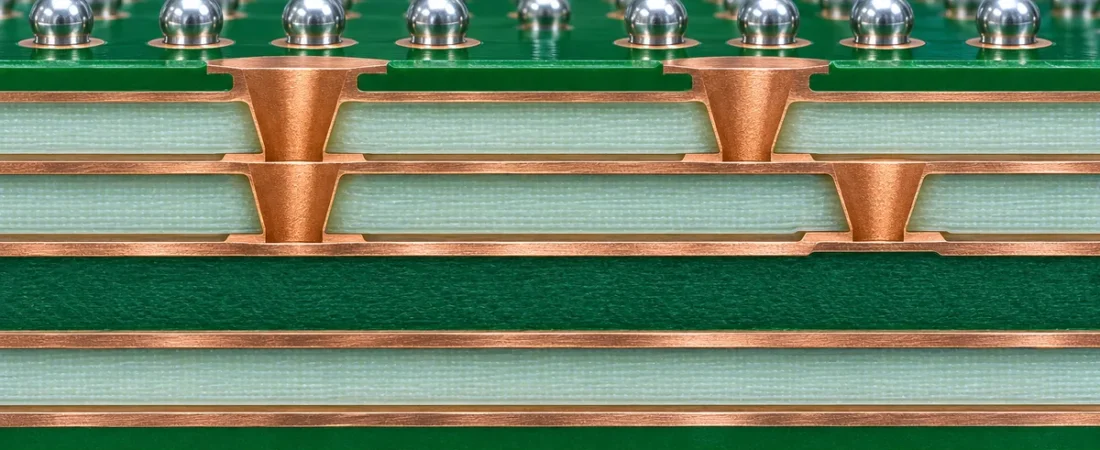
HDI does not simply mean using smaller holes. It changes how the PCB is built. A microvia layer is formed, plated and sometimes filled before another dielectric and copper layer can be added. When several microvia levels are required, the board may pass through repeated build-up and lamination cycles.
Stacked and staggered microvias can connect the same electrical layers, but they do not create the same manufacturing risk, routing freedom or cost. The right structure depends on BGA escape requirements, available pad area, dielectric thickness, copper-filling process, layer count and the reliability target.
1. Start with the required interconnection depth
A 1+n+1 construction has one build-up microvia layer on each side of a conventional core. A 2+n+2 construction has two microvia levels on each side and normally requires additional sequential processing. More levels increase routing density, but they also add material interfaces, registration steps and opportunities for cumulative variation.
| Construction | Typical connection need | Manufacturing implication |
|---|---|---|
| 1+n+1 | One microvia level from the outer layer to the next layer | Simpler build-up; often enough for many 0.5 mm-pitch escapes when the stack-up and routing permit. |
| 2+n+2 | Two microvia levels to reach the second internal build-up layer | More sequential processing and alignment control; stacked or staggered geometry must be defined. |
| 3+n+3 or deeper | Very high routing density or multiple layer transitions | Complexity and reliability review become critical; do not assume every supplier supports the same construction. |
The “n” in these descriptions is the conventional core section, not a universal number of layers. Final layer numbering, dielectric thickness and copper weights must be shown in the released stack-up.
2. Compare stacked and staggered microvias
Stacked microvias are vertically aligned. The upper microvia lands on the filled and planarised copper surface of the microvia below it. This saves lateral routing area, but it creates a direct metallurgical junction through the stack and normally requires reliable conductive filling and planarisation.
Staggered microvias are offset so each microvia lands on a separate capture pad connected by a short trace or copper feature. They consume more lateral space but avoid placing every via interface on one vertical axis. Where routing allows, industry guidance commonly prefers staggering over deep stacks.
| Decision factor | Stacked microvias | Staggered microvias |
|---|---|---|
| Routing density | Maximum vertical density; useful beneath very fine-pitch BGAs. | Needs lateral pad and connection space. |
| Via filling | Lower microvia generally needs copper filling and planarisation. | Lower via may not require the same stacked landing surface, subject to process. |
| Reliability exposure | Multiple aligned interfaces concentrate stress and require tighter process qualification. | Offset interfaces generally provide a less complex load path. |
| Cost and yield | Usually higher process complexity and tighter control. | Often the lower-risk choice if the layout can accommodate it. |
3. Sequential lamination drives more than lead time
Each build-up cycle can involve dielectric placement, lamination, laser drilling, desmear or surface preparation, metallisation, plating, via filling and planarisation before the next level is formed. The exact route depends on the selected material system and fabricator.
Extra cycles affect registration budget, material availability, panel throughput, inspection effort and scrap exposure. Two quotations that both say “HDI” may therefore describe very different constructions. Buyers should compare the released stack-up and process route, not only layer count and finished thickness.
4. Control the geometry and reliability assumptions
Microvia diameter, dielectric thickness and aspect ratio must be evaluated together. A small opening through an unnecessarily thick dielectric narrows plating access and the process window. Capture and target pads also need registration allowance; copying the smallest dimensions from a capability table can reduce yield without improving electrical performance.
For stacked structures, specify whether the microvias are copper filled, how the surface is planarised and how many stacked levels are qualified. Avoid stacking a deep microvia column on a buried via unless the fabricator has a qualified construction and the project evidence supports it.
| Release input | What must be explicit | Why it matters |
|---|---|---|
| Layer stack-up | Layer numbers, dielectric types and thicknesses, copper weights and finished thickness | Defines drilling depth, impedance context and lamination sequence. |
| Microvia map | Start/stop layers, diameter, pad sizes, stacked or staggered relationship | Prevents the CAM team from inferring the intended structure. |
| Fill requirement | Copper fill, planarisation and via-in-pad surface condition where applicable | Controls the landing surface for the next via or component pad. |
| Reliability evidence | Applicable class, thermal-stress or reflow requirement, coupon and microsection plan | Connects the construction to an agreed acceptance method. |
| Change control | Material or stack-up substitutions requiring approval | Protects impedance, registration and qualification assumptions. |
5. Ask for evidence that matches the risk
A microsection can confirm via geometry, copper fill, plating condition, registration and the interfaces between stacked levels. Thermal-stress or reflow testing can expose latent interconnect weaknesses, but the sample, cycle profile and acceptance criteria must be agreed before production. A generic certificate alone does not demonstrate that a new HDI stack has been qualified.
For an RFQ, send the native stack-up, Gerber or ODB++/IPC-2581 data, drill pairs, BGA pitch, impedance requirements and expected product class. JEXPCB can coordinate DFM review with the selected PCB process, but final dimensions should be confirmed against that process instead of copied from a generic online table.
Frequently asked questions
Are stacked microvias always unreliable?
No. Qualified two-level stacks are widely used. Risk rises when the stack becomes deeper, interfaces are poorly controlled or the design exceeds a proven process window.
Does every fine-pitch BGA require stacked microvias?
No. Package pitch, pad design, layer assignment and escape direction determine whether staggered or even single-level microvias are sufficient.
Can a fabricator change stacked vias to staggered during CAM?
Not without design approval. The change affects routing, pads, layer connectivity and potentially signal or power behaviour.
Technical references
- Global Electronics Association — IPC standards
- NCAB Group — Microvia design guidance
- Eurocircuits — HDI process development and cross-sections
References checked 14 November 2026. Final geometry, material, inspection and reliability requirements must be agreed with the selected fabricator.