
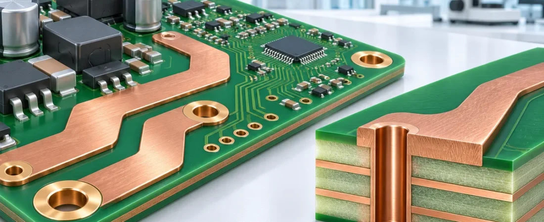
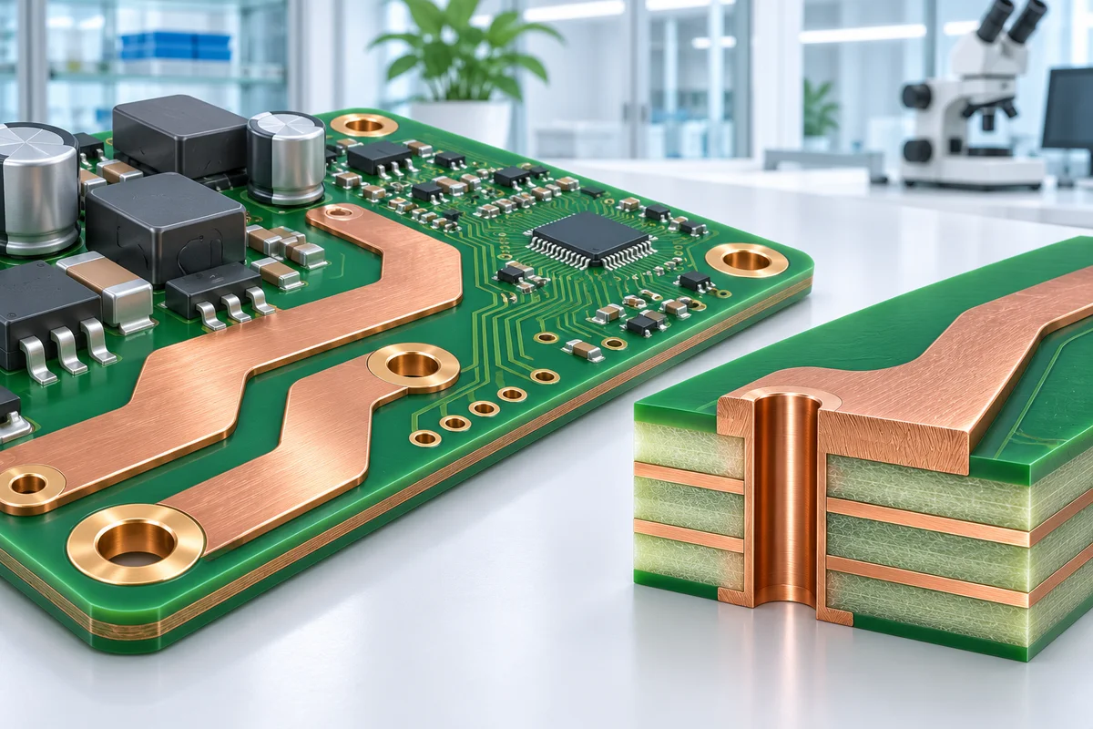
A thicker copper layer can reduce conductor resistance, but it also changes the fabrication window. A power board that looks straightforward at 1 oz may need wider isolation, a different stackup and a different assembly profile when copper thickness increases. Heavy copper is therefore a construction decision to agree before routing, rather than a last-minute purchasing option.
1. Specify the construction, not just an ounce value
The label heavy copper has no single purchasing threshold. State the required copper thickness on every layer and distinguish starting foil from finished copper. On outer layers, plating contributes to the final thickness; inner-layer foil follows a different process. Define tolerances, the governing specification and how conformance will be demonstrated. Do not assume that a board with thick planar copper also has equally thick copper in every hole barrel.
2. Recheck the manufacturing rules
Removing copper by etching creates lateral as well as vertical material loss. A geometry qualified for thin foil cannot simply be reused for thick foil. Ask the fabricator for rules for the actual construction, including conductor width, track-to-track and pad-to-pad spacing, annular rings and solder-mask coverage. Check fine-pitch connectors and control circuitry first: the power region may be easy while the smallest signal feature determines feasibility.
| Design decision | Confirm with manufacturing | Production consequence |
|---|---|---|
| Copper by layer | Starting and finished thickness; acceptance basis | Avoid mismatched quotations and an incorrect stackup. |
| Fine features | Width and isolation for the selected copper | Etching margin may require more board area. |
| Lamination | Dielectric build and resin filling around copper | Large copper steps need a qualified construction. |
| Solder mask | Coverage at copper edges and between pads | A thicker copper profile changes surface topography. |
| Assembly | Thermal reliefs and a measured soldering profile | Large copper areas can draw heat away from joints. |
3. Check the complete power path
For a simple conductor, resistance depends on resistivity, length and cross-sectional area. At the same current, resistive heating follows I²R. These relationships help compare options, but they do not produce a universal current rating. Ambient temperature, airflow, adjacent copper and the enclosure affect the result. Include neck-downs, terminals, fuses and layer transitions in the model; the narrowest or hottest connection can govern the board.
Use the actual minimum copper assumptions in the electrical and thermal analysis. Validate representative hardware under the intended continuous load and relevant transients. Do not assign a fixed current to every via or assume that adding identical vias gives ideal current sharing. A short thermal test in open air is not equivalent to the final enclosed product.
4. Release a buildable RFQ
Submit the layer stack, copper map, minimum feature sizes, finished board thickness, hole requirements and material constraints together. Identify high-current connections and any critical temperature or voltage-drop limits. Request a manufacturing review before design freeze and ask which changes require written approval. If fine routing and very high local current conflict, compare thicker foil with wider conductors, separate power sections or a qualified embedded-copper approach. Those alternatives require their own manufacturing and cost review.
Questions buyers ask
Does more copper always mean a cooler board?
No. It can reduce conductor loss, but heat still needs a path out of the assembly. Component losses, interfaces and the enclosure can dominate.
Can the factory increase copper after Gerber release?
Only after the construction and design rules are reviewed. A copper change can affect spacing, stackup, impedance and soldering.
Review copper thickness before freezing the layout
Send JEXPCB the proposed stackup and design constraints for a fabrication review. Agree the buildable construction and inspection requirements before comparing production prices.