
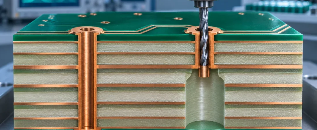
A plated through via does not stop electrically where a signal trace enters it. The unused barrel below or above that layer remains as a conductive stub, adding capacitance and creating a resonant discontinuity. At sufficiently fast edge rates or high channel bandwidth, the result can be extra return loss, insertion-loss ripple, jitter and a smaller eye opening.
Backdrilling—also called controlled-depth drilling—removes most of the unused copper barrel after plating. It can be highly effective, but it is not a default upgrade for every high-speed PCB. The decision should come from the stack-up, transition layers, residual-stub target and channel budget.
1. Understand where the stub is created
A through via connecting the top layer to an inner layer leaves the remaining plated barrel below the connection as an open-ended branch. The same issue appears from the opposite side when the transition ends before the barrel ends. Its impact depends on physical length, dielectric environment, drill geometry, return path and the signal spectrum—not only the advertised data rate.
| Transition | Unused barrel | Typical review |
|---|---|---|
| Top to bottom layer | Little or no stub | Backdrilling often adds limited value unless a connector launch or special structure creates another discontinuity. |
| Top to shallow inner layer | Long stub below the signal layer | Strong candidate for simulation and possible backdrilling on fast serial channels. |
| Bottom to shallow inner layer | Long stub above the signal layer | May require backdrilling from the top side. |
| Inner layer to inner layer | Unused barrel can remain on both sides | May require drilling from both sides or a different via structure. |
2. Decide from bandwidth and channel margin
There is no universal data-rate threshold. A long stub on a thick board can be harmful at a lower rate, while a short stub in a well-optimized transition may pass a higher-rate channel. Use the transmitter edge rate, required Nyquist/harmonic content, connector model, trace loss and receiver margin in pre-layout or post-layout simulation.
Backdrilling is most valuable when the via-stub resonance or added discontinuity materially consumes the channel budget. If the simulated and measured channel already has adequate margin, removing every stub may add cost and yield risk without a useful system benefit.
| Evidence | What it answers | Decision use |
|---|---|---|
| Stack-up and transition map | Which barrel section is electrically unused? | Calculates nominal stub and drilling direction. |
| 3D field or channel simulation | How does the transition affect S-parameters and the eye? | Tests alternative residual-stub targets before fabrication. |
| Interface/channel specification | What loss, return loss and eye margin are allowed? | Prevents a rule-of-thumb from replacing the actual budget. |
| Coupon or system validation | Does the manufactured structure match the model? | Closes the loop for production release. |
3. Specify the manufacturing target completely
Do not write only “backdrill high-speed vias.” Identify each via group, drilling side, target layer, finished hole size, backdrill diameter, maximum residual stub and minimum clearance to protected copper. State whether non-functional pads are removed and provide a drill legend or dedicated backdrill file.
The backdrill is normally larger than the original plated hole so it removes the barrel reliably. Its depth must stop before damaging the target pad or trace connection. Fabrication tolerance, board thickness variation, layer registration and drill-point geometry all consume the available depth window.
| Drawing item | Why it matters | Buyer check |
|---|---|---|
| Drill side and via group | Prevents drilling the wrong end or the wrong nets. | Match the legend, NC drill data and layer-transition list. |
| Residual-stub limit | Defines the electrical objective. | Use a realistic maximum with fabrication tolerance included. |
| Backdrill diameter | Must remove plating without violating nearby copper. | Review antipads, differential-pair spacing and breakout risk. |
| Target layer / stop depth | Protects the functional pad and trace connection. | Confirm stack-up thicknesses are released, not nominal guesses. |
| Verification method | Defines production evidence. | Agree on cross-section frequency, coupon or depth-control records. |
4. Design for fabrication margin
Provide enough clearance around the backdrilled barrel and do not place sensitive copper inside the supplier’s confirmed keepout. Very dense via fields, small pitch, sequential laminations and multiple backdrill depths can narrow the process window. Ask the fabricator to review manufacturability before freezing escape routing.
A small theoretical residual stub is not automatically better if it leaves almost no protection for the target layer. The optimum is the shortest stub that the approved stack-up and drilling process can produce repeatedly at acceptable yield.
5. Verify the finished board and release data
Cross-sections can show actual drill penetration, residual barrel, target-pad condition and registration. Electrical coupons or S-parameter measurements may be appropriate for critical channels, but the test method and acceptance limits must be defined in advance. Standard continuity testing alone does not prove that a stub meets the signal-integrity target.
Send the native stack-up, impedance table, high-speed net list, transition layers, drill files and any simulation-derived limits with the RFQ. JEXPCB can coordinate DFM review with capable PCB manufacturing resources; final depth capability and inspection plan should be confirmed against the selected production process.
Release checklist
| Input | Confirm before order | Evidence |
|---|---|---|
| Revision | Files, drawing and BOM use the same revision. | Controlled package or checksum. |
| Technical assumptions | Material, stack-up, process and acceptance criteria are explicit. | Reviewed quotation / DFM record. |
| Traceability | Required lot, process and inspection records are defined. | Traveler, report or certificate. |
| Change control | Deviation and substitution need named approval. | Written approval before production. |
Frequently asked questions
Does every PCIe or high-speed Ethernet board need backdrilling?
No. Need depends on edge rate, stack-up, transition depth, via geometry and channel margin. Simulate the actual structure.
Can blind or buried vias replace backdrilling?
Sometimes. They shorten the unused barrel but change lamination complexity, cost and reliability considerations. Compare the complete structure.
Is residual stub the same as drill-depth tolerance?
No. Residual stub is the remaining conductive barrel; depth tolerance is one contributor to its maximum value.
Can a finished board be backdrilled later?
It may be possible only when the design data, tooling and clearances support it. It should be planned before fabrication, not treated as a casual rework.
Technical references
- Samtec — Via Stubs: Practical Strategies to Mitigate Return Loss
- Samtec — Wideband RF Launches White Paper
- Siemens EDA — Accurate Via Stub Simulation
Technical references checked 5 November 2026. Project-specific simulation and the selected fabricator’s controlled-depth capability remain decisive.