
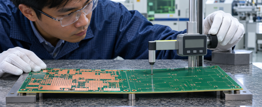
Copper balance is not a cosmetic CAM preference. It is part of the mechanical and electrochemical behavior of a printed circuit board. When copper is concentrated on one side of a layer, heavily biased between opposite layers, or distributed very differently across a production panel, the board can respond unevenly during lamination, etching, plating, solder-mask curing and assembly reflow. The visible result may be bow or twist, but the commercial consequence is usually broader: unstable solder-paste printing, placement-height variation, connector misalignment, selective-solder difficulty, fixture problems and avoidable disputes over acceptance.
This guide explains what PCB copper balance means, why copper distribution and stackup symmetry must be reviewed together, how poor balance affects fabrication and assembly, and what evidence engineering and purchasing teams should request before production release.
Do not approve a PCB only because every individual feature passes DRC. Review copper coverage by layer, the symmetry of the stackup, local copper density, panel-level distribution and the delivered bow-and-twist requirement as one connected manufacturing problem.
1. What does “copper balance” actually mean?
Copper balance describes how conductive copper is distributed within the board and production panel. It is not a single universal percentage limit. A useful review considers several related dimensions:
| Balance dimension | What to compare | Why it matters |
|---|---|---|
| Within one layer | Dense planes, large pours and connector fields versus open routing areas | Strong local density differences can influence etching, plating and local mechanical response. |
| Layer to layer | Copper coverage and copper weight on corresponding layers above and below the board centerline | Large asymmetry can create unequal stress as the multilayer construction heats and cools. |
| Stackup symmetry | Dielectric type, glass style, thickness and copper weight mirrored around the center | Balanced artwork cannot fully compensate for an inherently asymmetric material construction. |
| Panel distribution | Copper across repeated boards, breakaway rails, coupons and unused panel areas | The fabrication process acts on the production panel, not only on the finished outline. |
Two boards can show the same average copper coverage and still behave differently. A board with copper evenly dispersed may plate and move more consistently than one with an equally sized but highly concentrated copper block. Board size, thickness, aspect ratio, copper weight, layer count, laminate system, resin content, panel design and thermal history all affect the outcome. For that reason, a generic rule such as “keep every layer within a fixed percentage” should not replace project-specific CAM and stackup review.
2. Why uneven copper can produce bow and twist
FR-4 is a composite structure: copper, glass reinforcement and cured resin do not respond identically to temperature and processing. During multilayer lamination the stack is heated under pressure and then cooled. Later operations add further thermal and mechanical cycles. If the construction is materially or geometrically asymmetric, the two sides can develop different residual stresses. After the constraining pressure is removed—or after a later heat cycle—the panel may seek a new shape.
Bow is a roughly cylindrical or spherical departure from flatness while the corners remain essentially in one plane. Twist is a diagonal deformation in which one corner leaves the plane defined by the other three. IPC-TM-650 Method 2.4.22 describes production and referee procedures for determining bow and twist percentage on rigid boards and panels. The allowable value should come from the applicable procurement document, product standard and assembly need; it should not be assumed from an unrelated project.
Copper imbalance is only one contributor. An asymmetric stackup, mixed material behavior, resin-flow differences, pressing parameters, uneven cooling, panel geometry, moisture and later assembly heating can also influence flatness. This distinction matters during corrective action. Adding copper thieving to artwork may improve panel distribution, but it cannot automatically repair a poor stackup or an unsuitable production route.
3. The fabrication effects begin before the board reaches assembly
| Process stage | How imbalance can appear | Possible downstream effect |
|---|---|---|
| Etching | Very open and very dense regions load the etching process differently. | Process compensation becomes more difficult and conductor geometry may be less uniform. |
| Electrolytic copper plating | Current density is affected by pattern density, shielding and edge position. | Surface and hole copper distribution can become harder to control across the panel. |
| Lamination and cooling | Asymmetric copper and dielectric construction develops unequal residual stress. | Bow or twist may appear after pressing, routing or a later thermal cycle. |
| Solder-mask cure and surface finish | Additional heat cycles can reveal stress that was not obvious earlier. | A panel that looked acceptable at one checkpoint may move before final delivery. |
| Profiling and depanelization | Removing rails and tabs changes the mechanical constraint. | Finished-board flatness can differ from the supported production panel. |
This is why copper balance belongs in DFM, not only in final inspection. A finished board can pass continuity and still create process instability. Conversely, an isolated flatness measurement does not prove that copper distribution, plating uniformity or the stackup was well controlled.
4. How board flatness becomes an assembly problem
SMT equipment assumes that the board surface lies within a controllable process window. Warpage consumes that window at several steps:
- Solder-paste printing: a distorted board may not seal consistently against the stencil. Paste release and deposit height can vary, especially near unsupported or lifted areas.
- Component placement: local Z-height differences reduce placement consistency. Small passive components may be pressed too lightly or too heavily, while large packages can sit on uneven paste deposits.
- Reflow: thermal cycling can change the board shape again. For BGA, LGA and other area-array packages, relative movement between package and PCB can contribute to head-in-pillow, opens or nonuniform collapse when the entire assembly system is marginal.
- Through-hole and selective soldering: a bowed board may not locate or support consistently in pallets and fixtures; connector seating and lead protrusion can become less repeatable.
- Inspection and test: AOI focus, coplanarity assessment, bed-of-nails contact and mechanical fixture closure can all be affected by a board that does not sit predictably.
- Final integration: card guides, press-fit connectors, heat sinks, standoffs and enclosure interfaces can force a warped assembly flat, adding stress to solder joints and the laminate.
The risk is highest when several tolerances stack in the same direction: a thin or large board, one-sided component mass, an asymmetric layer construction, large copper planes on one side, dense area-array packages and tight mechanical interfaces. The correct response is not automatically a heavier fixture. Fixtures can control handling, but they do not remove the underlying material stress or guarantee the board will remain flat after depanelization and cooling.
5. Design actions that improve copper balance
Use a genuinely symmetric stackup where the product allows it
Mirror copper weights and dielectric thicknesses around the centerline, and review material types and glass styles with the PCB manufacturer. A layer count that looks symmetric on a drawing may still be materially asymmetric if dielectric constructions differ. High-current, RF, cavity, metal-backed and sequential-lamination designs may need intentional asymmetry; in that case the construction should be engineered and validated rather than treated as a normal stackup.
Distribute planes and pours instead of concentrating them unnecessarily
Large open areas next to dense copper regions deserve review. Ground or nonfunctional copper may help, but it must respect electrical clearance, creepage, controlled impedance, antenna keep-outs, high-voltage isolation, thermal design and test requirements. Copper added only for fabrication must never create an unintended electrical connection or alter the design authority’s approved function.
Coordinate copper thieving with the fabricator
CAM engineers may add isolated copper features in panel waste areas, around the circuit pattern or in rails to improve plating and distribution. The permitted locations, minimum clearance and ownership of CAM changes should be clear. For controlled-impedance or safety-critical products, review whether any added copper can affect coupling, dielectric spacing or certification constraints. Retain the approved production data or an auditable plot of supplier-added features.
Review the production panel, not only the single image
Mixed board designs, irregular outlines, large cutouts and unequal rail treatment can create a panel-level problem even when each board seems reasonable. Combine only compatible constructions in a panel, maintain adequate support, and review how coupons, tooling holes, fiducials, breakaway features and copper balancing patterns interact.
Do not use percentage coverage as a substitute for engineering judgment
CAM tools can report copper area by layer or region, which is valuable evidence. But the result must be interpreted in context. A global average can hide a dense corner, a broad unsupported opening or a strong top-to-bottom bias. Ask for coverage maps or zone analysis when the design is large, thin, heavy-copper, high-layer-count or mechanically sensitive.
6. A practical pre-release checklist
| Review item | Evidence to request | Release question |
|---|---|---|
| Stackup symmetry | Approved stackup with material family, dielectric thickness, copper weight and finished thickness | Is the build mirrored around the centerline, or is any asymmetry intentional and assessed? |
| Copper coverage | Layer-by-layer coverage report or CAM density map, including local hot spots | Are opposite layers and different panel zones reasonably balanced for this construction? |
| Supplier-added copper | CAM approval plot showing thieving, venting or balancing features and clearances | Has the design authority approved additions that could affect electrical or safety requirements? |
| Panel construction | Panel drawing with rails, coupons, tooling, fiducials, breakaways and board orientation | Will the panel remain mechanically stable through fabrication and assembly? |
| Flatness requirement | Specified standard, revision, board or array condition, test method and acceptance limit | Is acceptance defined for the delivered condition that the assembler will actually use? |
| Assembly validation | First-article records for paste print, placement, reflow, inspection, fixture fit and post-reflow flatness where relevant | Does the assembled process remain stable, not merely the incoming bare-board inspection? |
7. How to investigate a bow or twist problem
Start with facts from the same revision and lot. Record whether the distortion exists on the bare board, the production panel, after depanelization, after baking, after reflow or only after mechanical assembly. Identify the measurement method, sample support, temperature and moisture condition. Then compare:
- layer-by-layer copper coverage and local density maps;
- approved versus actual stackup and material lot;
- panel orientation, rail design, routing sequence and cooling method;
- reflow profiles, number of thermal cycles and board support;
- component mass and copper concentration on the top and bottom sides;
- flatness before and after each process stage.
A controlled comparison is more useful than attempting to flatten the same sample repeatedly. If a temporary straightening process is used, document it and verify that electrical, dimensional and reliability requirements remain satisfied. Straightening can change the shape; it does not explain the cause.
8. What JEXPCB needs for an effective review
For a project-specific copper-balance and manufacturability review, provide the current Gerber or ODB++ data, drill files, board outline, proposed stackup, finished thickness, copper weights, material requirement, impedance information, panel preference and the applicable bow-and-twist acceptance criteria. For assembly risk, also include the BOM, placement data, component-side drawings, reflow restrictions and critical mechanical interfaces.
JEXPCB can coordinate DFM, stackup and panel review through its manufacturing network and qualified partners before fabrication and PCBA assembly. The product owner should approve any change that can affect electrical behavior, safety spacing, controlled impedance, mechanical fit or qualification status. If the design is ready for review, submit the controlled file set through the PCB and PCBA quotation page.
Frequently asked questions
Does every PCB layer need exactly the same copper percentage?
No. Signal, plane and mixed layers serve different electrical purposes, and there is no universal percentage that guarantees success. The goal is a manufacturable distribution and mechanically sound construction, evaluated by layer, region, opposing-layer relationship and panel context.
Can the PCB manufacturer add copper thieving without approval?
The approved change process should define that authority. Copper added in nonfunctional or panel waste areas may be routine, but the fabricator must respect clearances and project restrictions. Any addition that could affect impedance, RF behavior, high-voltage spacing, thermal performance or certification should be reviewed by the design authority.
Will a symmetric stackup eliminate warpage?
It reduces one important source of risk but cannot eliminate all causes. Artwork distribution, materials, resin flow, lamination, cooling, panel geometry, moisture, reflow and assembly construction also influence flatness.
Should bow and twist be measured before or after assembly?
The required condition must be defined. Incoming bare-board inspection is useful, but a project may also need array-level, post-reflow or final-assembly verification. Use the applicable procurement document and test method, and state whether rails, components or fixtures are present.
Technical references
- IPC-TM-650 Method 2.4.22 — Bow and Twist (Percentage)
- Eurocircuits — Bow and Twist on a PCB
- Eurocircuits — The Influence of Copper Distribution on PCB Quality
- Sierra Circuits — Balanced Copper Distribution and Copper Weight in PCBs
Technical references checked 4 November 2026.