
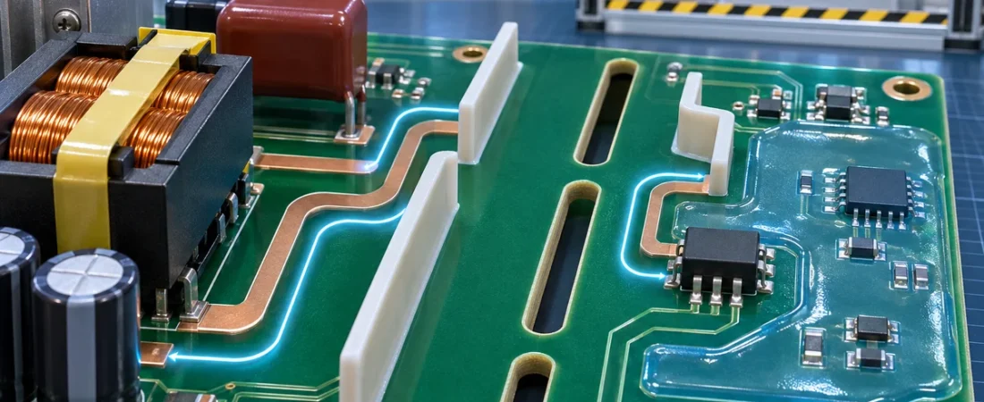
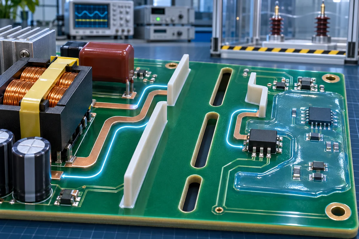
Clearance is the shortest distance through air between conductive parts. Creepage is the shortest path along an insulating surface. They respond to different failure mechanisms, so one number cannot replace the other.
At high voltage the required distance depends on working voltage, transient overvoltage, insulation type, pollution degree, altitude and the material’s tracking resistance. Product standards may override a generic table.
1. Convert product conditions into design inputs
Peak working voltage and transients affect clearance; RMS or working voltage, pollution and CTI/material group strongly affect creepage. Altitude reduces air dielectric strength.
| Input | Why it matters | Evidence |
|---|---|---|
| Working voltage | Sustained electric stress | Rated and worst-case circuit analysis. |
| Transient category | Impulse exposure | Product installation context. |
| Pollution degree | Surface contamination risk | Enclosure and environment definition. |
| Material group/CTI | Tracking resistance | Laminate recognition/data. |
| Altitude | Air breakdown strength | Maximum specified operating altitude. |
2. Use geometry carefully
A routed slot can lengthen a valid surface path and remove material from an air path, but only if width, depth and manufacturing tolerance are recognized by the governing standard. Solder mask alone is usually not treated as a dependable insulation barrier.
| Feature | Possible benefit | Design caution |
|---|---|---|
| Isolation slot | Longer path and physical separation | Board strength, copper pullback and router tolerance. |
| Barrier/rib | Extends surface path | Height and attachment must be controlled. |
| Copper keep-out | Protects actual minimum path | Include vias, pads, test points and edges. |
| Coating/potting | Reduces pollution exposure | Requires qualified material, coverage and process control. |
3. Verify after layout and assembly
The minimum path may be created by component leads, heatsinks, mounting hardware, connector shells or contamination, not only copper. Inspection must use the assembled state.
| Review stage | Check | Common miss |
|---|---|---|
| Schematic | Insulation boundary and fault energy | Wrong circuit separation. |
| PCB layout | 3D shortest paths and tolerances | Via or pad inside keep-out. |
| Assembly | Leads, solder, hardware, coating coverage | A component bridges the intended path. |
| Validation | Hi-pot/impulse and environmental tests as applicable | Testing only a bare board. |
Treat coating as a qualified process
Conformal coating can support reduced pollution exposure only where the relevant standard and certification allow it. Specify material, thickness/coverage, masking, cure, inspection, repair and production controls; “apply coating” is not a design rule.
Frequently asked questions
Does an isolation slot always increase clearance?
It can, but the standard’s measurement rules, slot dimensions and tolerances decide whether it is credited.
Can solder mask replace creepage distance?
Usually no. Do not assume ordinary solder mask is recognized insulation.
Should clearance be increased at altitude?
Often yes, because air dielectric strength falls; use the applicable altitude correction.
Technical references
- IEC 60664-1 — Insulation coordination
- UL Solutions — Printed wiring board materials
- Texas Instruments — High-voltage PCB design guidance
References checked 15 November 2026. Final distances must come from the applicable product safety standard and certified insulation system.