
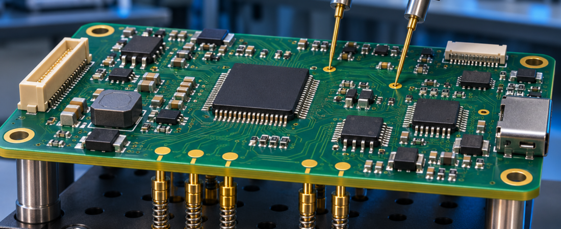
Design for test / PCB test-point planning
A PCBA cannot be tested efficiently if the test strategy begins after routing is complete. By then, critical nets may be hidden under BGAs, probe pads may be blocked by component bodies, programming access may be missing and the fixture may require avoidable complexity. Design for test (DFT) brings the test engineer, PCB designer and manufacturing partner together before layout release so that the board has the access, data and control features needed for the intended checks.
The practical rule: do not add test points until the team has defined what the production test must detect. Bare-board continuity, in-circuit test (ICT), flying probe, programming and functional test answer different questions. The layout should support the selected methods without degrading signal integrity, mechanical reliability or assembly yield.
1. Start with the defects and functions the build must verify
The first DFT decision is not pad diameter or pitch. It is the required evidence. A bare-board electrical test verifies continuity and isolation in the fabricated PCB before assembly. Assembly-level ICT and flying probe can detect accessible manufacturing faults such as shorts, opens, missing parts and selected component-value or polarity errors. Programming loads firmware or device configuration. Functional test checks specified behavior under defined power, stimulus, load and pass/fail limits.
| Method | Primary purpose | DFT input |
|---|---|---|
| Bare-board electrical test | Continuity and isolation of fabricated nets | Fabrication netlist, stackup and any special test requirements; dedicated assembly test pads may not be necessary. |
| ICT / bed-of-nails | Fast, repeatable access to many PCBA nodes | Stable probe locations, fixture-side access, mechanical support, program limits and fixture investment. |
| Flying probe | Flexible electrical access without a dedicated bed-of-nails fixture | Reachable pads, collision clearance, program data and acceptable cycle time. |
| Boundary scan | Digital interconnect coverage around supported devices where physical access is limited | Compatible devices, a correct JTAG chain, BSDL files and an executable test plan. |
| Programming | Load and verify firmware or configuration | Power, ground, clock/reset and programming-interface access plus file control and security rules. |
| Functional test | Verify specified board or product behavior | Firmware, connectors, loads, stimulus, limits, sequencing, safety and expected results. |
JEXPCB’s guide to AOI, X-ray, ICT and functional test explains the evidence each method provides. DFT is the earlier design activity that makes the selected electrical methods practical. One method does not automatically replace another: for example, a functional pass may not identify a wrong resistor, while ICT may not prove complete end-use performance.
2. Build a net-access strategy instead of adding pads indiscriminately
In an ideal low-density board, every relevant net could be probed. Modern density, high-speed constraints and package geometry often make complete physical access unrealistic. Keysight notes that loss of access is a major challenge for ICT, especially around dense packages, while boundary scan can recover some coverage when device support and test data are available. The design team and test engineer should therefore rank access before placement is frozen.
| Priority group | Typical nodes | Planning question |
|---|---|---|
| Power and return | Input rails, regulated rails, grounds, current-sense nodes and enable signals | Can the tester power safely, measure rails and isolate a short? |
| Programming and control | JTAG/SWD/UART/SPI programming, reset, boot straps and clocks | Can a blank unit be programmed and recovered without manual wiring? |
| High diagnostic value | Nodes that separate functional blocks or distinguish likely assembly faults | Will a failure localize to a component or remain a generic “board failed” result? |
| Analog and sensing | References, feedback, sensor inputs and measurement returns | Can these nodes be measured without loading or noise errors? |
| Digital interconnects | Buses, memory interfaces and device-to-device connections | Is physical probing suitable, or should boundary scan or functional coverage be used? |
| Field diagnosis | Service rails, debug interfaces and critical status signals | Is a durable loop, header or labelled pad needed beyond production test? |
A test point is not useful merely because it exists in the CAD file. It must expose the intended electrical node on the assembled board and remain reachable after soldering, coating, shielding and mechanical assembly. A via designated for test becomes unusable if solder mask tents it. A pad under a component may be available for bare-board testing but inaccessible after placement.
3. Treat probe access as a mechanical interface
Altium’s test-point documentation recommends defining the allowed test side, pad/via eligibility, spacing, component clearance and board-edge clearance with the fabricator and assembler. These rules are equipment-dependent. Avoid copying a universal pad size or pitch from another project; obtain the actual fixture and flying-probe design rules before layout release.
Choose the access side early. Keeping automated test points on one side can simplify the fixture. Two-sided probing may recover coverage but can increase fixture complexity, alignment requirements and cost. The decision also affects where tall components, shields, heat sinks and connectors may be placed.
Provide a clean landing surface. A probe needs exposed, planar and repeatable metal. Confirm the permitted surface finish, solder-mask opening, pad geometry and whether a via hole is acceptable. Do not place silkscreen, adhesive, conformal coating or solder-mask residue in the contact area.
Protect collision and support zones. Probe bodies are wider than their tips. Clearance must account for nearby components and their maximum height, not only copper-to-copper spacing. Edge distance, tooling holes, datum features and board support also matter. Bed-of-nails fixtures can apply the combined force of many spring probes, so the support plate and probe distribution must limit flexing around thin areas, BGAs and cutouts.
Make identification unambiguous. Use stable test-point designators and coordinates in the released data. Human-access points for prototype debugging may also need readable labels, but do not assume a silkscreen label alone identifies the net in the test program.
4. Add access without damaging the circuit being tested
Test structures add copper, capacitance, inductance and stubs. On low-speed rails this may be negligible; on RF, high-speed serial, clock, precision analog and high-impedance nodes it may change the behavior being measured. The test engineer should define the required measurement, while the electrical designer decides whether a direct pad, series isolation, controlled connector, built-in test function or non-contact method is appropriate.
- Avoid uncontrolled stubs: do not branch a long trace to a convenient pad on a high-speed net without signal-integrity review.
- Plan safe power injection: separate fixture power, sense and return paths where accuracy or current is important; define current limits and sequencing.
- Control board state: provide a repeatable way to hold processors, converters, radios and outputs in a safe test mode.
- Protect sensitive nodes: confirm probe loading, ESD handling and maximum stimulus before exposing references, sensor inputs or RF circuits.
- Provide isolation when needed: removable links, zero-ohm options, test switches or boundary-scan control may make a shared node diagnosable.
DFT must be reviewed together with design for manufacturing. A test pad that violates solder-mask dams, paste printing, creepage, impedance or component-placement rules is not an acceptable solution.
5. Match the access pattern to the production test method
ICT: a bed-of-nails fixture offers repeatable parallel contact and short cycle times, which can suit a stable higher-volume product. It requires fixture design, stable coordinates and enough accessible nodes. The layout should be frozen before the fixture is built; even a small revision can invalidate probes, supports or the test program.
Flying probe: moving probes avoid a dedicated nail bed and can be attractive for prototypes, new-product introduction or changing builds. It still needs accessible surfaces and collision-free motion. Coverage, test time and contact reliability depend on the board, program and equipment. “No fixture” does not mean “no DFT.”
Boundary scan: IEEE 1149.1/JTAG-compatible devices can test selected interconnects that are difficult to reach physically. Keysight emphasizes that correct BSDL data, chain implementation and access to required control points are critical. Boundary scan does not cover unsupported analog parts or every fault by itself.
Functional test: connector-level access can reduce dedicated pads, but the specification must define inputs, outputs, loads, timing, firmware, calibration and pass/fail limits. A functional station should also provide enough diagnostics to distinguish a manufacturing defect from firmware, configuration or setup problems.
6. Release a complete test package and run a formal DFT review
| Release item | Useful content |
|---|---|
| Design identity | PCB/PCBA part number, revision, approved BOM and assembly variant. |
| CAD and net data | ODB++/IPC-2581 or agreed fabrication/assembly data, netlist, centroid and drawings. |
| Test-point list | Unique designator, net name, X/Y coordinate, side, pad type and allowed use. |
| Mechanical definition | Board outline, thickness, tooling holes, keepouts, component heights and support restrictions. |
| Electrical test specification | Power sequence, current limits, stimuli, measurements, tolerances, test modes and safety. |
| Programming package | Approved image, version, device configuration, interface, verification and serialization rules. |
| Coverage record | Required nets/functions, covered method, known exclusions and approved risk disposition. |
| Failure handling | Diagnostic outputs, retest rules, golden-board control and repair/traceability requirements. |
Run the DFT review before layout release, then repeat it after routing and before fixture commitment. The review should use the manufacturing partner’s current equipment rules and the actual PCBA variant. Confirm that all required pads remain exposed, reachable and correctly mapped; that probe force can be supported; that programming and test files are under revision control; and that expected coverage gaps are documented rather than discovered during pilot production.
Common avoidable failures: selecting ICT after layout completion, relying on pads hidden by components, tenting test vias, omitting ground or reset access, placing points too close to tall parts, changing the PCB after fixture build, and supplying a test-point file whose net names or coordinates do not match the released revision.
Technical references
- Keysight — In-Circuit Test for Manufacturing.
- Keysight — Flying Probe Testing vs. In-Circuit Testing.
- Keysight — ICT Boundary Scan Development Steps.
- Teradyne — In-Circuit Testing.
- Altium — Assigning Testpoints on the Board.
Planning test access for a new PCBA?
JEXPCB can review test objectives, layout access, programming requirements and manufacturing data before release, then coordinate the appropriate fabrication, assembly and project-specific test flow.