
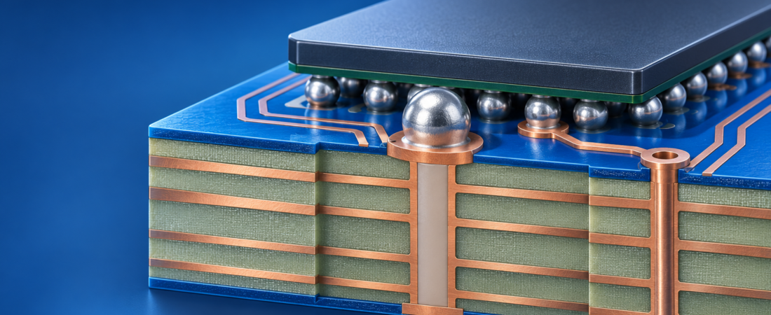
PCB Manufacturing / Via protection
“Via-in-pad” describes where a via is placed, not how the hole is finished. An open, tented, plugged, filled or copper-capped via can look similar in a layout but behave very differently during fabrication and soldering. When a via sits inside a BGA, QFN or other surface-mount pad, the fabrication notes must define the required structure before the PCB is released.
Do not write only “fill vias.” Identify exactly which vias require treatment, whether the fill is conductive or non-conductive, whether the surface must be planarized and copper capped, which side or sides are treated, and what finished surface must accept solder.
1. Tented, plugged, filled and capped are not interchangeable
IPC-4761 defines several via-protection structures. The standard distinguishes tenting, plugging, filling, covering and metal capping because each method addresses different manufacturing risks. A supplier should not have to infer one term from another. [1]
| Structure | What it means in practice | Typical limitation |
|---|---|---|
| Open via | The plated hole remains exposed. | Solder, flux or chemistry can enter or pass through the hole. |
| Tented / covered via | Solder mask or another covering closes the surface without completely filling the barrel. | The cover may not create a flat, solderable component pad. |
| Plugged via | Material is introduced into part of the via depth. | “Plugged” does not mean completely filled or metal capped. |
| Filled via — Type V | The barrel is filled with an agreed conductive or non-conductive material. | The exposed surface is not automatically suitable as an SMT land. |
| Filled and covered — Type VI | A filled via is covered with a dry-film or liquid coating on one or both sides. | The covering is different from a plated copper cap. |
| Filled and capped — Type VII | The via is filled, planarized and metallized over to form a flat copper surface. | It adds process steps, cost and acceptance requirements. |
For a solderable via-in-pad, a filled-and-capped structure is commonly specified. IPC technical guidance recommends Type VII protection when via-in-pad is required. The applicable design, acceptance and reliability requirements still need to be agreed for the specific product. [2]
2. Why an untreated via inside a pad creates assembly risk
Via-in-pad can shorten the escape path, save routing space and support dense BGA or HDI layouts. It can also reduce the discontinuity introduced by a longer dog-bone connection. These benefits are most valuable when component pitch and available routing channels make conventional fan-out difficult. [3]
The same geometry places the via directly under solder paste or a solder ball. If the hole remains open, molten solder can wick into the barrel during reflow. The pad may then receive less solder than intended, increasing the risk of an insufficient joint or voiding. A depression, exposed resin or incomplete cap can also disturb pad planarity. Under a BGA, these defects are difficult to see by normal visual inspection.
Via-in-pad is therefore not a layout-only decision. It links PCB drilling, plating, filling, planarization, copper capping, surface finish, stencil design and assembly inspection. The board fabricator and assembler should review the same requirement before production.
3. Non-conductive fill, conductive fill or solid copper?
Non-conductive epoxy is often the baseline choice
A non-conductive epoxy fill blocks solder movement and supports planarization without being selected primarily as an electrical conductor. It is widely used for plated-over via-in-pad structures. The via barrel still carries the electrical connection through its copper plating; “non-conductive fill” does not mean the via becomes electrically non-conductive.
Conductive fill is not automatically better
Conductive fill may be considered where the design requires a specific thermal or current-carrying result, but material properties, expansion behaviour, process capability and cost must be reviewed. For demanding thermal structures, solid copper-filled or plated microvias may be available. These options should be chosen from measured design needs rather than from the assumption that a conductive fill is always more reliable. [4]
Stacked microvias need a separate reliability review
HDI designs may use staggered or stacked microvias. The number of lamination cycles, microvia geometry, copper filling method, target reliability class and inspection plan can materially change manufacturability. Do not apply one generic via-fill note to through holes, blind vias and stacked microvias unless the supplier confirms that the same requirement is appropriate.
4. What to specify before PCB production
Put the requirement in the fabrication drawing or controlled specification and make the affected holes unambiguous in the drill data. A separate drill layer or clearly identified tool table can help distinguish via-in-pad holes from ordinary vias.
- Location and scope: identify the pads, via types and board sides that require treatment.
- Finished geometry: define finished hole, pad, capture pad, annular ring and drill span; include microvia stack or stagger information.
- Protection type: state the agreed IPC-4761 type where applicable, instead of using “plug,” “fill” and “cap” as synonyms.
- Fill material: specify conductive, non-conductive epoxy or another approved process, including any material restriction.
- Surface condition: require complete fill, planarization and copper cap where a solderable pad is needed; agree acceptable dimpling, protrusion or void criteria.
- Final finish and mask: define the surface finish and solder-mask geometry for the component land.
- Verification: agree electrical test, visual or X-ray inspection, microsection sampling and documentation when required by product risk.
Also ask whether the selected via size, aspect ratio and copper cap are within the fabricator’s qualified process window. A capability value on a general table does not replace a DFM review of the actual stackup and pad geometry.
Questions to close during DFM review
| Question | Why it matters |
|---|---|
| Could dog-bone fan-out meet the density and signal requirements? | A conventional via may reduce process cost when space allows. |
| Are the via size and pad geometry compatible with filling and capping? | Insufficient capture or annular ring can create registration and plating risk. |
| Which vias need Type VII and which only need tenting or covering? | Treating every via the same can add cost without adding value. |
| How will the filled surface be inspected? | Planarity, cap integrity and internal fill quality need agreed evidence. |
| Does the assembler know the final pad structure? | Stencil, reflow and X-ray decisions depend on the actual solderable surface. |
Before release, compare the fabrication drawing, drill files and component footprint. Conflicting notes such as “tent all vias” and “copper-filled via-in-pad” should be resolved by revision, not left for CAM engineering to interpret. Explore our PCB fabrication service or send the design for a DFM review.
Common questions
Does every via-in-pad need conductive fill?
No. Non-conductive epoxy is commonly used when the main objectives are to stop solder wicking and create a planar, plated surface. Conductive or solid-copper options should be tied to defined thermal or electrical requirements.
Is solder-mask tenting enough under a BGA pad?
Tenting is not equivalent to a filled, planarized and copper-capped solderable land. For a via located directly in a component pad, confirm the required finished structure with both the PCB fabricator and assembler.
- IPC — IPC-4761 via-protection types
- IPC — Via-protection selection guidance
- Sierra Circuits — HDI PCB design guide
- TTM Technologies — HDI and microvia structures
References checked 3 November 2026. Examples are educational and do not represent universal capability limits. Confirm the applicable standard revision, acceptance criteria and qualified process with the selected production site.
Clarify the via structure before the PCB is released.
Share the Gerber files, drill data, stackup and component requirements. We can coordinate a DFM review of via-in-pad, filling and capping requirements before quotation or production.
Request a QuoteRelated Articles
HDI Microvias: Stacked vs Staggered Vias and Sequential Lamination
A practical HDI guide to stacked and staggered microvias, sequential lamination, reliability trade-offs and production-release data.
Thermal Via Design for Power Components: Placement, Size and Solder-Wicking Risks
A practical guide to thermal-via placement, diameter, pitch, plane connection, filling and assembly trade-offs.
PCB Backdrilling: When Via Stubs Become a Signal-Integrity Risk
A practical engineering guide to via-stub risk, backdrill decisions, manufacturing tolerances and inspection evidence for high-speed PCBs.